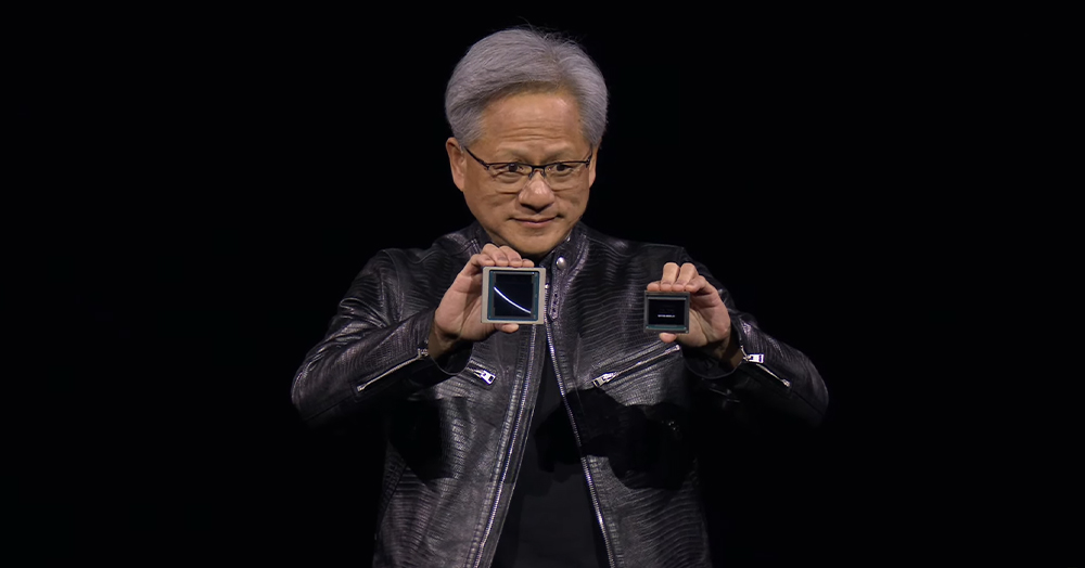
Reports indicate that Nvidia has invested a sum of $10 billion in developing the Blackwell architecture.
Despite the hefty cost of this project, the expected financial returns will help achieve a solid yield on this large investment.
CEO Jen-Sun Huang announced the Blackwell architecture and B200 graphics processing unit, described by Nvidia as the next generation of data center and artificial intelligence graphics processing units, delivering a massive leap in computational capacity for future generations.
The B200 graphics processing unit succeeds the H100 and H200 units, in addition to the GB200 Superchip graphics processing unit, which, as its name suggests, will retain the design of the Grace CPU central processing unit and also include a graphics processing unit from the Blackwell architecture.
Nvidia is expected to unveil the GB202 graphics processing unit from the Blackwell architecture in the RTX 50 series of cards in 2025, which will be completely different from data center models in terms of design.
Nvidia’s B200 graphics processing unit is the first to adopt a multi-chip module (MCM) design, housing two GPUs inside the same chip.
According to a report from Teh Kim, a prominent writer for Barons magazine, Nvidia has made a massive financial investment in developing the Blackwell architecture. The company aims to achieve significant financial returns, as Jen-Sun Huang stated in his interview on CNBC that the cost of purchasing the B200 graphics processing unit ranges from $30,000 to $40,000, a significant increase compared to prices of graphics processing units based on the Hopper architecture.
While companies like AMD hold some market share in the artificial intelligence (AI) processing sector, Nvidia still dominates strongly in this field.


